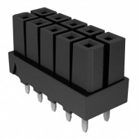
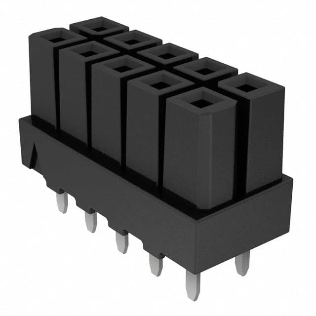
The Samtec IPBS-105-01-T-D is a 10-position, dual-row, 0.165-inch (4.19mm) pitch pin header, finished with a matte tin plating. While it appears as a simple interconnect, a thorough interpretation of its datasheet is critical for reliable design. This guide will dissect the key parameters and application considerations for this specific component.
Key Electrical Specifications and Their Practical Meaning
The primary electrical specification for this header is its current rating, typically listed as 3.0 to 4.0 Amps per pin, depending on the specific test conditions (e.g., 30°C temperature rise at 80% of rated current). In practice, this means you should not expect to draw 4A from every pin simultaneously in a real-world assembly. The rating is often derived from a single pin being energized in free air. When all 10 pins carry current, mutual heating will reduce the safe operating current. A prudent design rule is to derate this component to 2.5 Amps per pin for continuous operation in a typical 50°C ambient environment. The contact resistance is another vital parameter, typically specified as 10 milliohms maximum. This low resistance ensures minimal voltage drop and power dissipation (I²R losses) at the junction. However, this value can increase over time due to oxidation or fretting corrosion, especially with tin plating which is prone to forming a non-conductive oxide layer. The tin's "wiping" action during mating breaks through this oxide, but repeated thermal cycling or vibration can degrade the connection. The dielectric withstanding voltage (e.g., 500 VAC RMS) indicates the insulation capability between adjacent pins. This is crucial for high-voltage applications but does not imply the component can be used at that voltage continuously; it is a short-term test parameter. The insulation resistance (typically 1000 megohms minimum) ensures very low leakage current between pins under dry conditions.
Absolute Maximum Ratings and Derating Considerations
The absolute maximum ratings are stress limits that must never be exceeded, even momentarily. For the IPBS-105-01-T-D, the operating temperature range is usually -55°C to +125°C. Exceeding this can cause the thermoplastic housing to soften (above 125°C) or become brittle (below -55°C), leading to mechanical failure. The peak current rating is higher than the continuous rating but must be applied with a low duty cycle, typically less than 1% and for durations under 1 second. Derating is the engineering practice of operating the component well below its absolute maximum to ensure reliability. For this header, the most critical derating is thermal derating. The current rating is inversely proportional to ambient temperature. At 85°C ambient, you should reduce the current by approximately 20-30%. A second derating factor is altitude. At higher altitudes (above 10,000 feet), the reduced air density lowers the dielectric breakdown voltage, so the voltage rating should be halved. Finally, consider derating for multi-row loading. With two rows of 5 pins each, the center pins will run hotter than the edge pins. A common practice is to limit the total current to 80% of the sum of individual pin ratings.
Typical Application Circuit Analysis
This header is rarely used as a standalone component; it is part of a larger circuit. In a typical application, it serves as a board-to-board connector, a wire-to-board connector (when mated with a socket like the Samtec IPSS series), or a programming header. For a power distribution scenario, the pins are often paralleled to increase current capacity. For example, if you need 10A, you might allocate three pins for VCC and three for GND, leaving four for signals. The datasheet does not explicitly show this, but analyzing the pin layout (2x5 matrix) suggests a symmetric pinout is beneficial for minimizing voltage drop. In a high-speed signal application (e.g., for a SPI or I2C bus), the header introduces parasitic inductance and capacitance. The pin-to-pin capacitance is typically around 1 pF, and the inductance is in the low nanohenry range. This can cause signal degradation at frequencies above 10 MHz. The datasheet may not provide S-parameters, but you can infer from the 0.165-inch pitch that it is not optimized for high-frequency signals. You should place a series resistor (e.g., 22 ohms) near the driving pin to dampen any ringing caused by the connector's parasitic elements.
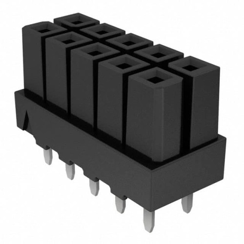
Pin Configuration and Package Considerations
The pin configuration is a standard 2x5 grid with a 0.165-inch (4.19mm) pitch between pins and rows. The polarization is achieved by a physical key or notch in the housing, ensuring the mating socket cannot be inserted incorrectly. The pins are square (0.025-inch square post) which provides good retention force. The mounting style is through-hole, meaning the pins are soldered into plated through-holes on the PCB. This offers excellent mechanical strength compared to surface mount versions. The PCB footprint should have a hole diameter of about 0.040 inches (1.02mm) to accommodate the pin with a tight interference fit. The standoff height (the distance from the PCB surface to the bottom of the plastic housing) is typically 0.100 inches (2.54mm). This is critical for cleaning flux residues after wave soldering. The housing is made of a high-temperature thermoplastic (e.g., LCP or PPS) rated for lead-free soldering processes up to 260°C peak.
Thermal Management Guidelines
Although a connector is not a power component like a MOSFET, thermal management is still essential because the contact resistance generates heat. For the IPBS-105-01-T-D, the primary heat source is the I²R losses at the pin-to-socket interface. In a 10-pin header carrying 3A per pin, the total power dissipation could be 10 (3² 0.01) = 0.9 watts. This heat must be conducted away through the PCB traces. To manage this, ensure that the copper traces connected to each pin are wide enough (at least 0.100 inches for 3A) to act as heat sinks. For high-current pins, use a thermal relief pattern for the through-hole pads to facilitate soldering, but do not use a full isolation pad which would trap heat. The datasheet may not provide a thermal resistance value (theta-JA), but you can assume a junction-to-ambient thermal resistance of roughly 50-60°C/W for the entire header in still air. This means a 0.9W dissipation would raise the internal temperature by about 50°C above ambient, which is acceptable for most applications. If multiple headers are placed close together, add a 10-20% derating factor to account for cumulative heating.
How to Read and Interpret Characteristic Curves
The datasheet for this header typically includes a current derating curve showing maximum current versus ambient temperature. This curve is a straight line that starts at 4A at 20°C and drops to 0A at 125°C. Interpret this by noting that the current rating is not constant; it is tied directly to the housing's temperature capability. A second common curve is the temperature rise vs. current plot. This is an exponential-like curve where a small increase in current beyond the rated point causes a disproportionate rise in temperature. For example, 3A might yield a 20°C rise, but 4A could cause a 35°C rise. Use this curve to find the safe operating point for your specific duty cycle. There may also be a contact resistance vs. number of mating cycles curve. This shows a gradual increase in resistance after 500 or 1000 cycles due to tin wear. For high-reliability applications (e.g., frequent programming), expect the contact resistance to double after 200 cycles. There is typically no timing diagram for a passive connector, but if the header is part of a matched impedance system (e.g., for LVDS), the datasheet may provide a characteristic impedance plot (e.g., 50 ohms) versus frequency. This is derived from the physical geometry and is critical for signal integrity analysis in high-speed digital designs.