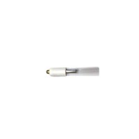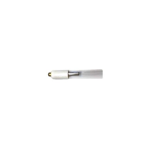
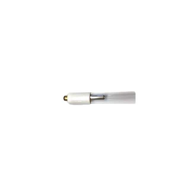
The FOR ATLANTIC ULTRAVIOLET 05-0094, supplied by Interlight under SKU WW-0BTC-8, is a specialized ultraviolet (UV) light source designed for disinfection and curing applications. To ensure reliable performance and longevity, careful attention must be paid to the driving circuit, passive component selection, and PCB layout. This application note provides practical guidance for design engineers integrating this component into their systems.
Recommended Circuit Topologies and Design Best Practices
The 05-0094 is a UV lamp that requires a controlled ignition and steady-state current. The most robust topology is a half-bridge resonant inverter, often referred to as an electronic ballast. This topology provides efficient AC power conversion, low electromagnetic interference (EMI), and inherent current limiting. The resonant tank, consisting of a series inductor (L) and capacitor (C), shapes the current waveform to be sinusoidal, which is ideal for the lamp’s life. A DC-to-AC inverter with a DC link voltage of approximately 310V (from a rectified 230VAC input) is typical. Design best practices include implementing a preheat phase: before striking the lamp, apply a high-frequency, low-voltage current for one to two seconds to warm the filaments. This dramatically extends lamp life. Following preheat, a resonant voltage boost (via frequency sweeping) initiates the arc. Once the lamp is lit, the control loop must regulate the lamp current to its rated value, typically between 300-500mA depending on the specific lamp variant. A microcontroller with a dedicated PWM output driving a half-bridge gate driver is the recommended control method, allowing precise frequency and duty cycle control.
Component Selection Guidelines for Supporting Passives
The resonant inductor must be a ferrite-core type designed for high-frequency operation (20-100 kHz typical for UV ballasts) and must handle the peak resonant current without saturating. Select an inductor with a saturation current rating at least 20% higher than the expected peak current. The resonant capacitor should be a polypropylene film capacitor (MKP or similar) with a low dissipation factor and a voltage rating of at least 1.5 times the peak voltage across it (often exceeding 1kV during ignition). For the DC link, use electrolytic capacitors with a ripple current rating sufficient for the ballast’s input current, and a voltage rating of 450V for 230VAC inputs. The output capacitors (if used for filtering) should be X7R or C0G ceramic types for stability. All passive components must have a rated temperature range of -40°C to +105°C to suit industrial environments. Ensure the MOSFETs in the half-bridge have a VDS rating of at least 600V and a fast body diode to handle the resonant switching.
PCB Layout Recommendations and Routing Tips
The PCB layout is critical for both performance and safety. Begin by placing the high-voltage components (DC link capacitors, MOSFETs, resonant tank, and lamp connector) in a separate, isolated area from the low-voltage control circuitry. Use a dedicated ground plane for the power stage, and a separate, star-connected ground for the control section, joining them at a single point near the input filter. Keep the high-current loop (DC link to MOSFETs to resonant tank and back) as short and wide as possible to minimize stray inductance and resistance. For the resonant inductor, place it at least 5mm away from any sensitive analog traces to avoid magnetic coupling. The high-voltage traces to the lamp connector should be routed with a minimum clearance of 3mm from other traces and the board edge, and should be covered with a thick solder mask (or use a conformal coating) to prevent arcing. Use a thermal relief pattern on pads connected to large copper pours to facilitate soldering. For the control signals (PWM, feedback), use short, direct traces and avoid running them parallel to high-voltage lines.
EMC/EMI Considerations and Mitigation Strategies
The resonant switching of the half-bridge generates conducted and radiated EMI. The primary mitigation strategy is a robust input EMI filter. Place a common-mode choke (e.g., 10-20 mH) and two X-class capacitors (e.g., 0.1 µF and 0.47 µF) between the AC input and the bridge rectifier. A ferrite bead on the DC link line can suppress high-frequency noise. For radiated EMI, use a grounded metal enclosure or shield can over the ballast circuit. The PCB itself should have a solid ground plane on one layer to act as a shield. Ensure that the resonant tank components (L and C) have their own local ground connection to the power ground plane. To reduce differential mode noise, the resonant switching frequency should be kept above 20 kHz (the audible range) but below 150 kHz where conducted emissions limits are more stringent. If needed, add a small snubber (a series RC network, e.g., 10 Ω and 100 pF) across each MOSFET to dampen ringing. Finally, ensure the lamp wires are twisted and kept as short as possible to minimize antenna effects.
Common Design Pitfalls and How to Avoid Them
One frequent mistake is undersizing the resonant capacitor voltage rating, leading to catastrophic failure during ignition. Always verify the peak voltage with an oscilloscope during prototyping. Another pitfall is ignoring the lamp’s end-of-life behavior—when a UV lamp reaches its end of life, the arc voltage can rise, causing the current to drop. A simple current-sense resistor in series with the lamp, monitored by the microcontroller, can trigger a shutdown or warning. Do not operate the lamp without a proper preheat phase; cold starting drastically reduces lamp life. A third pitfall is poor thermal management of the MOSFETs and inductor. Use a heatsink for the MOSFETs and ensure adequate airflow around the inductor. Finally, avoid using a single ground plane for both power and control; this invites ground bounce and instability. Implement a star-ground topology as mentioned.
Prototyping Tips and Bench Testing Procedures
Begin prototyping on a breadboard for the control circuit only, but transfer the power stage to a perfboard or a custom PCB with proper copper traces. Always use a current-limited power supply (set to 50% of the expected input current) during initial testing. Use a high-voltage differential probe for measuring lamp voltage and a current probe for lamp current. Start with the preheat phase only, verifying the filament current and duration. Next, test the ignition sequence with a dummy load (a 100kΩ resistor in series with a 10nF capacitor) before connecting the actual lamp. Once the lamp is lit, monitor the lamp current waveform to ensure it is sinusoidal and stable. Check for excessive ringing on the MOSFET drain-source voltage; adjust the snubber values if necessary. Finally, run the system for at least 24 hours to verify thermal stability and component life. Use a thermal camera to spot hot spots. For EMC pre-compliance, use a near-field probe to identify radiating sources and apply ferrite beads or shielding as needed.