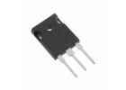
The Infineon IRF100P219AKMA1 is a robust 100V N-channel MOSFET in the TO-247AC package, designed for high-efficiency power conversion in applications such as switched-mode power supplies (SMPS), DC-DC converters, motor drives, and battery management systems. Its low on-resistance (Rds(on)) and fast switching characteristics make it ideal for both hard-switched and resonant topologies. For most designs, a half-bridge or full-bridge topology is recommended to leverage the MOSFET’s low gate charge (Qg) and body diode performance. In a synchronous buck converter, this device serves as the high-side and low-side switch, requiring careful dead-time management to avoid shoot-through. For boost or flyback converters, use it as the primary switch with a snubber network to clamp voltage spikes. A gate driver IC with at least 2A peak current capability is essential to achieve fast switching transitions and minimize switching losses. Always place a low-ESR ceramic capacitor (e.g., 10µF to 100µF) as close as possible to the drain-source terminals to absorb high-frequency ripple and stabilize the input voltage.
When selecting supporting passive components, choose a gate series resistor (Rg) between 5Ω and 22Ω to control switching speed and mitigate ringing. For bootstrap diode in half-bridge configurations, use an ultrafast recovery diode rated for at least 100V and 1A forward current to ensure reliable charge replenishment. The bootstrap capacitor should be a low-ESR ceramic type with a value of 1µF to 10µF, placed right at the high-side gate driver supply pin. For sense resistors in current-mode control, use a 1% tolerance, low-inductance resistor (e.g., metal-strip or thick-film) rated for the peak current. Snubber components, typically a series RC network (e.g., 1Ω resistor and 1nF capacitor), should be placed across the drain-source or across the transformer primary to dampen oscillations. Always derate capacitors and resistors by at least 20% for voltage and power to account for temperature and aging effects.
PCB layout is critical for achieving the MOSFET’s rated performance and reliability. Place the IRF100P219AKMA1 as close to the input bulk capacitor as possible to minimize stray inductance in the high-current loop. Use a dedicated power plane for the drain connection and a separate copper pour for the source return path, ensuring the loop area for the switching current is as small as possible. The gate drive trace should be kept short (under 10mm) and routed away from high-dV/dt nodes to prevent parasitic coupling. Use Kelvin source connections for the gate driver return path to avoid sharing the high current path, which can induce false turn-on. For the TO-247AC package, ensure the tab (drain) is soldered to a large copper area for thermal dissipation, and use multiple vias (at least 6-8, 0.5mm diameter) to connect top and bottom layers for heat spreading. Avoid routing sensitive analog traces near the MOSFET’s drain or gate terminals.
To manage electromagnetic compatibility (EMC) and electromagnetic interference (EMI), implement a snubber network across the MOSFET’s drain-source to suppress voltage ringing at turn-off, which is a primary source of conducted and radiated emissions. Use a ferrite bead in series with the gate drive output to filter high-frequency noise without slowing switching too much. A common-mode choke on the input power lines, combined with X-capacitors (e.g., 0.1µF rated for 250VAC), helps filter differential mode noise. Place a Y-capacitor (2.2nF to 4.7nF) between the primary and secondary ground in isolated converters to shunt common-mode currents. Optimize the switching speed by adjusting Rg; slower switching reduces EMI but increases losses, so find a balance through iterative testing. Use a shielded inductor or transformer to contain magnetic fields, and keep the high-frequency loop (drain-source-capacitor) area under 1cm².
Common design pitfalls include inadequate gate drive voltage—ensure Vgs is between 10V and 12V for full enhancement, as lower voltages increase Rds(on) and thermal stress. Another frequent mistake is ignoring the body diode reverse recovery; in hard-switched topologies, the diode’s Qrr can cause excessive losses and EMI. Mitigate this by using a Schottky diode in parallel (if voltage margin allows) or by implementing zero-voltage switching (ZVS). Thermal runaway can occur if the MOSFET is not properly heatsinked; always attach a TO-247AC-compatible heatsink with thermal paste or a pad, and verify junction temperature stays below 125°C under worst-case conditions. Avoid routing gate traces parallel to drain traces to prevent Miller effect-induced turn-on. Finally, never exceed the maximum drain-source voltage (100V) even during transients; use a TVS diode or clamp circuit if necessary.
For prototyping, use a double-sided or four-layer PCB with ample copper thickness (2oz recommended) to handle high currents. Begin bench testing with a low-voltage, low-current power supply (e.g., 20V, 1A) to verify gate drive waveforms and switching behavior without risking device failure. Use an oscilloscope with a high-voltage differential probe for drain-source measurements and a current probe for drain current. Measure the gate-source voltage at the MOSFET pins to confirm clean transitions (under 50ns rise/fall time) and no oscillations. Perform a double-pulse test to characterize switching losses and body diode performance. Gradually increase the input voltage and load current while monitoring temperature with a thermal camera or thermocouple. Finally, run a full-load burn-in test for at least one hour to validate thermal stability and EMI compliance. Document all waveforms and temperatures for future reference.