Introduction to the Component
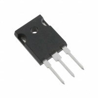
The STPSC20H065CW is a dual Schottky diode array in a TO-247 package, featuring a 650V reverse voltage rating and a 20A forward current capability per diode (40A total). Manufactured by STMicroelectronics, it leverages silicon carbide (SiC) technology, which offers superior switching performance and thermal efficiency compared to standard silicon diodes. This component is ideal for high-frequency power conversion circuits, such as boost converters in power factor correction (PFC) stages, due to its near-zero reverse recovery charge and low forward voltage drop. In this tutorial, you will design a continuous conduction mode (CCM) boost PFC rectifier using this diode array, making it a practical choice for learning about high-voltage, high-efficiency power design.
Design Requirements and Specifications
Your circuit will be a 1kW CCM boost PFC stage operating from a universal AC input (85-265Vrms, 50/60Hz) and delivering a regulated 400V DC output. Key specifications include: output power (P_out) = 1000W, input voltage range (V_in_min = 85Vrms, V_in_max = 265Vrms), output voltage (V_out) = 400V DC, switching frequency (f_sw) = 100kHz, and maximum efficiency >95% at full load. The STPSC20H065CW must handle the peak diode current and reverse voltage stress without failure. The design will focus on selecting the boost inductor, output capacitor, and control IC while ensuring the diode array operates within its safe operating area (SOA).
Step-by-Step Design Process with Calculations
First, calculate the peak input voltage at minimum AC input: V_in_peak_min = 85V sqrt(2) = 120V. The maximum input current occurs at minimum input voltage: I_in_max = P_out / (V_in_min efficiency PF) = 1000W / (85V 0.95 0.99) ≈ 12.5A rms. The peak inductor current is I_L_peak = I_in_max sqrt(2) + 0.5 delta_I, where delta_I (ripple current) is typically 20-40% of peak input current. Choose delta_I = 30%: I_L_peak = 12.5 1.414 + 0.5 (0.3 12.5 1.414) ≈ 17.7A + 2.65A = 20.35A. The STPSC20H065CW’s per-diode current rating of 20A is adequate, but you should derate for temperature: at 100°C case temperature, the current rating drops to about 14A per diode. Since the diodes operate in parallel (common cathode), total current capability is 28A, providing margin. The boost inductor value is L = (V_in_min D) / (f_sw delta_I), where duty cycle D = (V_out - V_in_peak_min) / V_out = (400 - 120)/400 = 0.7. Thus, L = (120V 0.7) / (100kHz 2.65A) ≈ 317µH. Choose a standard value of 330µH. The output capacitor must handle hold-up time: C_out = (2 P_out t_hold) / (V_out^2 - V_out_min^2), with t_hold = 20ms and V_out_min = 350V: C_out = (2 1000W * 0.02s) / (400^2 - 350^2) ≈ 40 / (160000 - 122500) = 40 / 37500 ≈ 1067µF. Use two 560µF, 450V electrolytic capacitors in parallel.
Component Selection Rationale for the Complete BOM
The STPSC20H065CW is selected for its low forward voltage (1.5V at 20A, 25°C) and zero reverse recovery, which minimizes switching losses at 100kHz. For the boost switch, choose a 650V SiC MOSFET like the STW40N65M5 (40A, 0.099 ohm R_ds_on) to match the diode’s high-speed capability. The boost inductor (330µH) should use a Kool Mu or Sendust core to handle high flux without saturation; a commercial option like the Coilcraft SER2918H-333. The output capacitors are Panasonic EEU-FC2G561 (560µF, 450V, low ESR). For the control IC, the UCC28019 (Texas Instruments) is a good fit for CCM PFC with integrated protection. Add an EMI filter with a common-mode choke (e.g., Würth 744825170) and X-class capacitors (0.47µF, 275VAC) to meet EN55022 Class B. A heatsink for the TO-247 package, such as the Aavid 529802B02500, with a thermal resistance of 2°C/W, ensures the diode junction stays below 125°C at full load.
Simulation Tips and What to Look For
Use LTspice or SIMetrix to simulate the CCM PFC stage. Model the STPSC20H065CW with its SPICE subcircuit from STMicroelectronics. Key waveforms to examine: diode current and voltage during switching transitions; ensure the reverse voltage never exceeds 650V (including spikes due to parasitic inductance). Look at the diode’s junction temperature by integrating its power loss (P_loss = V_f * I_avg + switching losses). At 100kHz, switching losses should be minimal (<1W) due to SiC’s fast recovery. Monitor the inductor current for CCM operation—it should not go to zero during the AC cycle. Adjust the control loop bandwidth to 10-20Hz for stable PFC output. Simulate startup and load transients (e.g., 10% to 100% load step) to verify the output voltage overshoot is <5% (under 420V).
Prototype Build and Testing Methodology
Construct the circuit on a 2-layer PCB with a copper thickness of 2oz to handle high currents. Place the STPSC20H065CW on the heatsink using thermal paste and a mica insulator. Connect the anode pins to the boost inductor and the common cathode to the output capacitor. For testing, use a variable AC source (Variac) with an isolation transformer and a DC load (e.g., Chroma 63804). Start with no load and slowly increase the AC input to 85Vrms while monitoring the output voltage. Verify the PFC control IC regulates V_out to 400V. Gradually add load up to 1000W, checking the diode case temperature with a thermocouple (keep below 125°C). Use a current probe (e.g., Tektronix TCP0030) on the diode anode to observe its switching waveform—look for clean turn-off without ringing. Measure input power with a power analyzer (e.g., Yokogawa WT310) to calculate efficiency: expect >95% at full load.
Performance Verification and Optimization
Verify the power factor (PF) at full load: should be >0.99 at 230VAC input and >0.95 at 85VAC. Measure total harmonic distortion (THD) of input current—aim for <10%. If efficiency is below 95%, check the heatsink thermal resistance; consider adding forced air cooling (e.g., a 40mm fan) to reduce diode junction temperature. Optimize the gate drive for the SiC MOSFET: a gate resistor of 10 ohms reduces ringing without excessive switching loss. Adjust the boost inductor value if the ripple current is too high—increase L to 470µH to reduce core losses. For the diode array, ensure the two internal diodes share current equally; measure each diode’s forward voltage drop at full load—they should be within 10% of each other. If not, add small series resistors (0.1 ohm) to balance current. Finally, perform a 24-hour burn-in test at 1000W to confirm reliability. The STPSC20H065CW’s rugged SiC structure ensures long-term stability, making this design suitable for industrial power supplies.