Introduction to the LTM4609IY
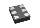
The LTM4609IY from Analog Devices is a complete, high-efficiency step-down (buck) DC-DC converter module that accepts an input voltage from 4.5V to 34V and delivers an adjustable output from 0.8V to 34V at up to 4A continuous current. What makes this component particularly suitable for a hands-on tutorial is its integrated inductor, power switches, and compensation circuitry in a compact 15mm x 15mm LGA package. This significantly reduces the external component count and simplifies the design process, allowing you to focus on the core principles of power supply design without getting bogged down in the complexities of magnetic component selection and feedback loop compensation.
Design Requirements and Specifications
For this practical circuit, we will design a 12V output supply from a 24V industrial input rail. The target specifications are: input voltage range 18V to 30V (nominal 24V), output voltage 12V ±1%, output current 3A (with 4A peak), output ripple less than 50mV peak-to-peak, and efficiency greater than 85% at full load. The operating temperature range is -40°C to +85°C.
Step-by-Step Design Process with Calculations
Step 1: Set the Output Voltage
The output voltage is programmed by a resistor divider from the VOUT pin to the FB pin. Use the formula: VOUT = 0.8V x (1 + R1/R2). Choose R2 = 10.0kΩ (a standard 1% value). Then R1 = (VOUT/0.8V - 1) x R2 = (12/0.8 - 1) x 10.0k = (15 - 1) x 10.0k = 140kΩ. Use a standard 1% value of 140kΩ (or 140kΩ exactly).
Step 2: Determine Input Capacitance
The input capacitor must handle the ripple current. For a buck converter, the RMS ripple current is approximately IOUT x sqrt(D x (1-D)), where D = VOUT/VIN = 12/24 = 0.5. At 3A, IRMS ≈ 3A x sqrt(0.5 x 0.5) = 1.5A. Use two 22µF, 50V ceramic X7R capacitors (e.g., Murata GRM32ER71H226KE18) in parallel to handle the ripple and provide low impedance.
Step 3: Select Output Capacitance
The output capacitor determines ripple and transient response. A good starting point is 100µF total. Use two 47µF, 16V ceramic X7R capacitors (e.g., TDK C3225X7R1C476M) plus a 10µF in parallel. This gives low ESR and good high-frequency decoupling.
Step 4: Set the Switching Frequency
The LTM4609 operates at a fixed 800kHz. No external frequency-setting resistor is needed. For noise-sensitive applications, you can synchronize it to an external clock via the SYNC pin, but for this tutorial we use the default frequency.
Step 5: Soft-Start and Tracking
The SS pin controls soft-start time. Connect a capacitor to ground: CSS (nF) = tSS (ms) x 1.3. For a 5ms start-up, use CSS = 5 x 1.3 = 6.5nF, use a standard 6.8nF capacitor. Leave the TRACK pin floating for independent operation.
Component Selection Rationale for the Complete BOM
The complete bill of materials is minimal. Input capacitors: Two 22µF/50V X7R ceramic (low ESR, high ripple rating). Output capacitors: Two 47µF/16V X7R plus one 10µF/16V X7R (total 104µF, low ESR for low ripple). Feedback resistors: One 140kΩ and one 10.0kΩ, both 1% tolerance to ensure output accuracy. Soft-start capacitor: 6.8nF, X7R or COG. Optional components: A 10µF/50V ceramic at the input for high-frequency bypass, and a 0.1µF ceramic at the output for noise. The LTM4609IY itself is the core component. No inductor or diode is needed, as these are integrated.
Simulation Tips and What to Look For
Use LTSpice (free from Analog Devices) with the LTM4609 model. Simulate the circuit with a 24V input and 3A resistive load. Key waveforms to observe: Output voltage start-up (should ramp linearly over 5ms), output ripple (should be less than 10mV at steady state due to ceramic caps), switch node voltage (should show clean 800kHz square wave between 0V and VIN), and input current ripple (should show the typical buck waveform). Vary the input from 18V to 30V and check output regulation stays within 1%. Add a load transient (e.g., 0.5A to 3A step) and observe output deviation—expect less than 100mV. If oscillations occur, check input/output capacitor ESR or add a small series resistor (0.1Ω) to the output capacitor.
Prototype Build and Testing Methodology
Build the circuit on a two-layer PCB with a solid ground plane. Place the LTM4609IY centrally, with input and output capacitors as close as possible to the respective pins (<5mm). Keep the feedback trace short and away from noisy switch nodes. Use 2oz copper for high current paths. For testing, connect a variable DC supply (18-30V) to the input through a current-limited supply (set to 5A). Connect an electronic load or power resistor (e.g., 4Ω for 3A at 12V) to the output. Start with no load, apply input, and verify output voltage is 12V ±0.12V. Increase load gradually to 3A while monitoring output voltage with an oscilloscope (AC-coupled, 20MHz bandwidth limit). Check for ripple and stability. Use a thermal camera to check component temperatures—the LTM4609 should stay below 85°C at 3A with natural convection.
Performance Verification and Optimization
Measure efficiency at 24V input: Efficiency = (VOUT x IOUT) / (VIN x IIN). Expect >90% at 3A. If below 85%, check for excessive input ripple (add more input capacitance) or output ripple (add a small 1µF ceramic). For improved transient response, increase output capacitance to 200µF. For lower noise, add an LC output filter (1µH + 10µF). Finally, test over temperature by heating the board to 85°C in a chamber and verifying output regulation. The LTM4609IY’s integrated design makes this a robust and repeatable power solution, perfect for engineers wanting a practical, high-performance DC-DC converter without the complexity of discrete designs.